A Simple Way to Test Buck Converter Stability
AN075
This application note offers a detailed guide on the assessment of converter stability. For designers, it is important to consider the application of fast load steps to converters and monitor output voltage responses to identify potential issues. In fact, different buck converters with their compensation networks can have different solutions to address ringing in load step response. At the end of this article, a simple and useful, Li-Ion battery-powered DIY tool for creating fast load steps will be introduced.
1 Time Domain Analysis
The common way to check converter stability is via frequency domain analysis, by measuring the open loop frequency response, and observing the control loop cross-over frequency and phase margin at the cross-over point. It is a complicated measurement, requiring specialized expensive equipment. A simpler way to quickly check converter stability is via time domain analysis by applying a fast load step to the converter and observing the output voltage response during the load step: It will highlight potential problems regarding loop stability, input supply stability, slope compensation issues, load regulation and layout problems.
|
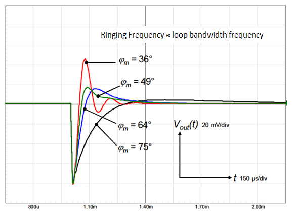
Figure 1
|
The step-load response in Figure 1 shows several converter loop stability cases, from very stable (phase margin 75°) to very unstable (phase margin 36°). It can be seen that any ringing in the step-load response indicates too low phase margin, and this increases the tendency towards oscillation.
It is important to realize that the speed (rise time) of the load step should be much faster than the control loop speed of the converter in order to see these instability effects. Step-loads with rise/fall times of 200 ~ 500nsec will be sufficient to test the stability of most buck converters.
|
|
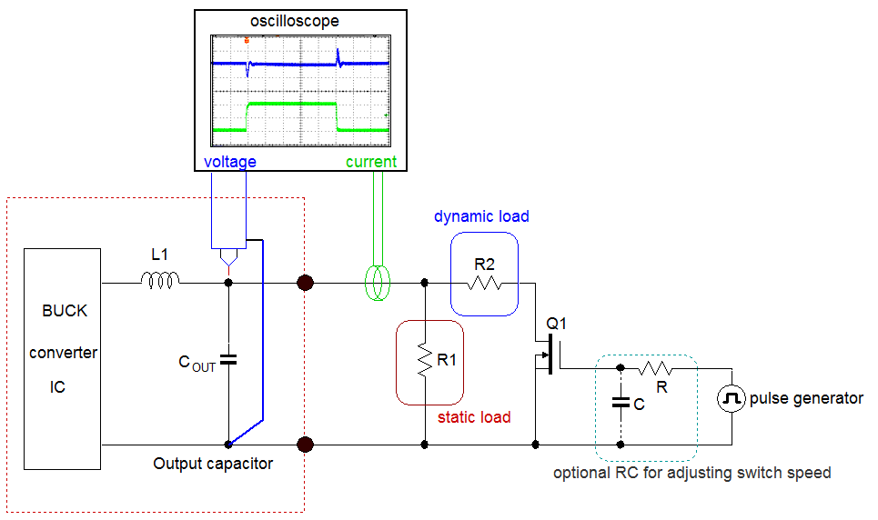
Figure 2
|
Figure 2 shows a simple tool to generate fast load steps to a converter: A MOSFET driven by a pulse generator switches a load resistor on and off at the converter output. A fixed resistor provides the static load. The load current is measured via current probe and the converter output voltage is measured directly at the converter output capacitor. With this setup, load-step rise and fall times of 500nsec can be easily reached.
|
|
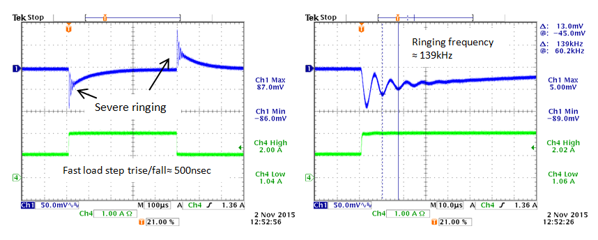
Figure 3
|
Figure 3 shows an example of a fast load step response with excessive ringing.
It is possible to estimate the converter cross-over frequency my measuring the step load ringing frequency. This can be helpful in finding the reason for the instability.
|
2 How to Improve Ringing
Current mode buck converters with Gm type error amplifiers have compensation network connected to ground.
|
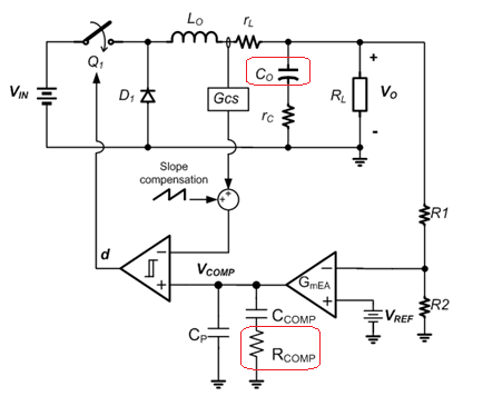
Figure 4
|
The converter loop bandwidth is approximated by:
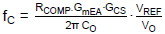 , where fC is normally around 1/10 – 1/20 of the switching frequency. , where fC is normally around 1/10 – 1/20 of the switching frequency.
If the measured cross-over frequency is much higher that the value calculated by the formula, the reason for the deviation must be found.
In many cases the MLCC output capacitor value may be lower than the rated value because of capacitance drop due to higher DC bias or lower ACRMS ripple voltage. If that is the case, either increase the output capacitance (adding more capacitors) or reduce RCOMP, which will both lower the converter bandwidth. See Figure 4.
|
|
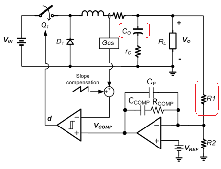
Figure 5
|
Current mode buck converters with OPAMP type error amplifiers have compensation network connected as shown in Figure 5.
Loop bandwidth is given by: 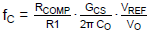
Buck converter ICs with internal compensation often use this configuration.
It is important to realize that the value of the feedback resistor R1 plays a role in the converter stability. Too low values for R1 will result in too high cross-over frequency and will lead to low phase margin and ringing in step-load response.
|
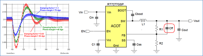
Figure 6
The Richtek new generation 18V rated ACOT® parts like RT6252A/RT6252B, RT6253A/RT6253B, RT6262A/RT6262B, RT6263A/RT6263B, RT6264A/RT6264B behave in the same manner as RT7277 stability wise.
2.1 ACOT® Buck Converter Stability
Richtek ACOT® converters don’t have an error amplifier as they operate in ripple based hysteretic control mode.
ACOT® converters can show ringing in load step due to insufficient damping of the hysteretic control loop. This often happens in applications with higher output voltage or high duty-cycles. Larger output capacitance also increases the chance of output ringing. To increase the damping of the control loop, add Cff as shown in Figure 6.
The optimal value for Cff can be derived from the ringing frequency: 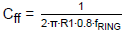 .
.
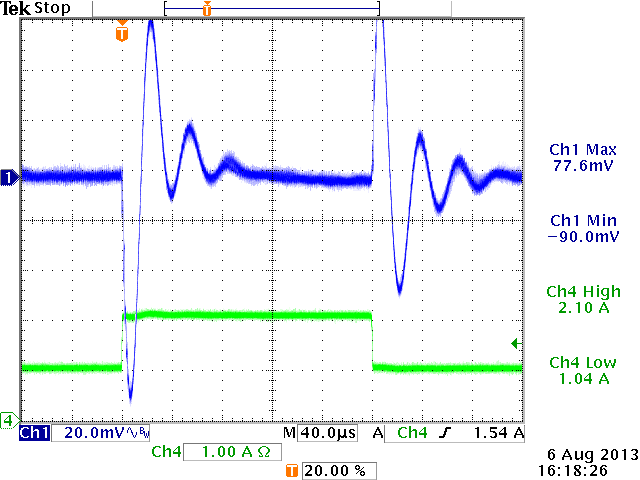
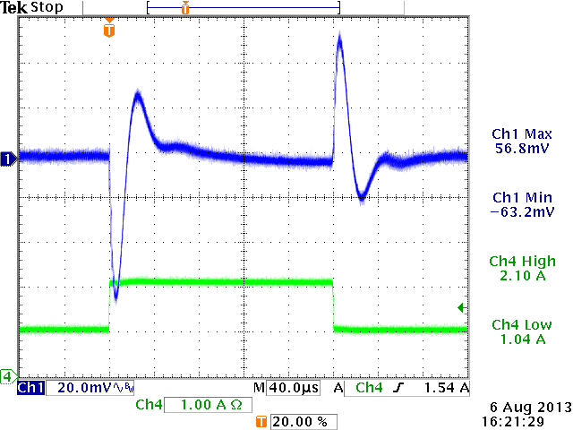
The measurements below show an example of a 5V application with different Cff values.
|
5V application: Cout = 44µF
|
|
Cff = 0pF
|
Cff = 33pF
|
Cff = 82pF
|
|
|
|
|
Other reasons for ringing in step-load response: Input supply ringing.
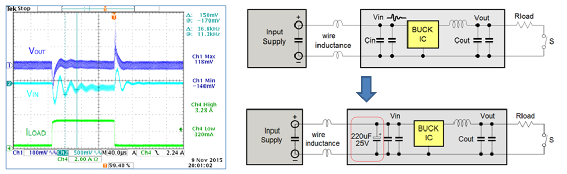
A load step at converter output will also result in a load step at the converter input. If the input supply has stability problems, or there is inductance in the input supply wires, the instability or resonance at the input supply can be visible on the output rail as well. Resonance problems at the input supply can be solved by adding an electrolytic capacitor parallel to the converter MLCC input capacitor. It will act as an RC snubber and damp the input ringing.
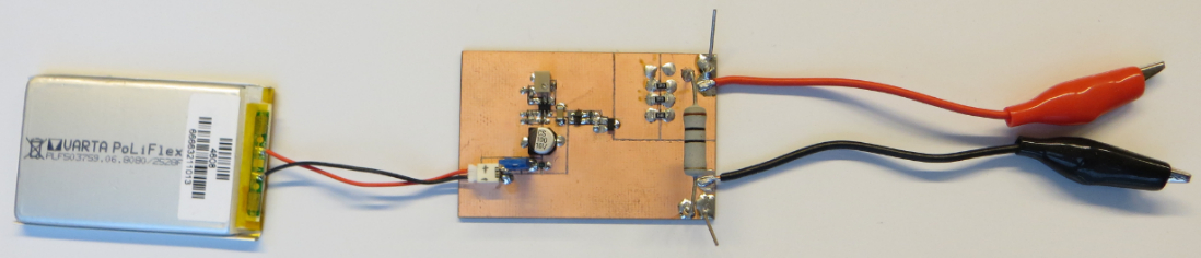
3 Example of a Simple DIY Portable Load Transient Tool
A practical solution for a flexible fast transient tool is shown in the schematic in Figure 7:
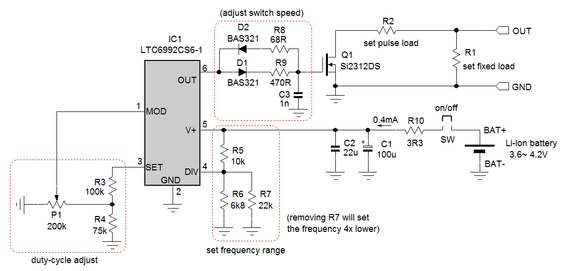
Figure 7
IC1 is a voltage controlled PWM generator IC. The voltage on the MOD pin sets the PWM duty-cycle, the voltage on the DIV pin sets the frequency range, and the resistor value connected to the SET pin sets the precise frequency. The OUT pin has sufficient driving capability to drive small MOSFETs with fast rise and fall times. The duty-cycle is normally set at a low level, around 5%. This makes it possible to draw larger pulse currents while limiting the total power in the pulse load resistor and MOSFET. A pulse width of around 150µsec is sufficient to see the full voltage sag and recovery in most DC/DC converters, so the PWM frequency can be set at around 330Hz.
It is most convenient to power the circuit via a Li-Ion battery; this makes the circuit fully isolated and avoids ground bounce between grounded equipment. The circuit is designed in such a way that battery voltage variations will not impact frequency or duty-cycle settings, and with a current consumption of only 0.4mA, the battery life is very long.
For more information, please read the full application note Buck Converter Stability Testing
To stay updated with more information about our products, please subscribe to our newsletter.